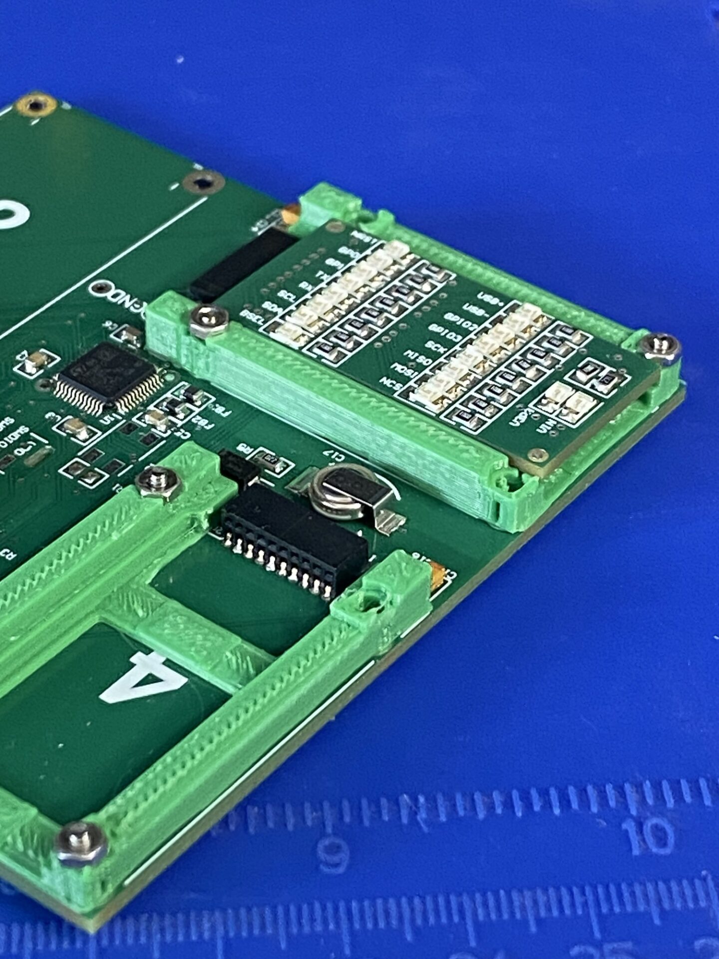
Most of my work involves rapid prototyping, so for electrical engineering purposes, it’s great to have component-level building blocks that can be snapped together in different configurations. One problem with most building-block approaches like MikroBus (which is really pretty great, BTW) is that they are aimed at hobbyists – they don’t carry over well to production. It would be great to take a rapidly-prototyped design directly to manufacturing without having to re-spin the design.
I struggled with other shortcomings in the bus ecosystem. Some buses like MikroBus are good for IoT but lacking in mid-speed or high-speed comms. Some require expensive connectors or uncommon PCB requirements. Many are just too inflexible, having gone through the standards gauntlet.
Since I couldn’t find a bus I liked, I started tinkering – and thus NanoSlot entered the world.
I have been evolving NanoSlot for a few years now and I’ve been turning out new designs faster than I would have believed possible just a few years ago. NanoSlot is really great for IoT projects, embedded devices, component evaluations – or just plain messing around, if that’s your thing.
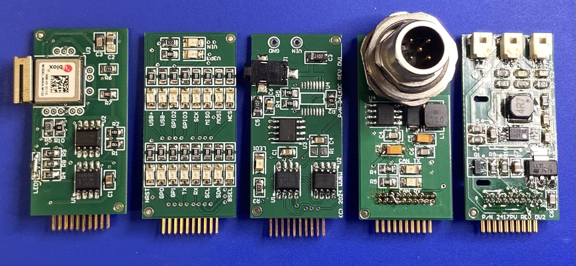
What is NanoSlot?
NanoSlot is loosely defined – it’s not a rigid specification, but rather a flexible set of mechanical, electrical, and software guidelines. The goals?
- Enable rapid prototyping
- Prototype to production capabilities – fewer respins, better mechanicals, simplified assembly wherever possible
- Holistic approach to hardware+software – modules can carry their software and settings with them
- Good mixture of connectivity including GPIO, I2C, SPI, USB, serial, and multiple power rails
- Flexible standards – rigidity being the enemy of creativity
- Processor agnostic – while I might favor one MCU vendor, this is not required
- Operating system agnostic – again, some may be preferred, but none shall be excluded
- Form Factor Freedom – Hosts and modules can combine horizontal and vertical geometries to suit many applications
- “The Ultimate Evaluation Kit” – new chips can be mounted on a module along with their eval firmware, allowing designers to get a module and evaluate components in minutes
This article is meant to be an intro and not a spec sheet, so I’ll keep this discussion informal. I’m writing up the hard specs as they evolve, and they will be available for free on the website, of course.
NanoSlot mechanicals
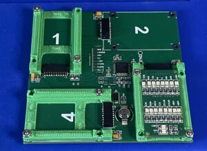
Physically, NanoSlot is very free-form. Generally a design will consist of a host (which may or may not have a CPU or MCU, and can be a passive backplane) that sports one or more bus connectors for add-in modules. Modules can be attached horizontally or vertically, and modules are fabricated from commonly available 0.062” PCB stock, in as many layers as desired. This keeps proto PCB runs cheap and fast.
Components can be mounted on both sides, with some limitations. There are altitude guidelines (especially for modules used in horizontal-mount hosts, of course), but there are no hard restrictions.
Early versions of NanoSlot used an edge-card approach, but high-speed connectors in both horizontal and vertical orientations for 0.062” PCBs are pricey. (The Samtec HSEC8 line worked really well, but often times the cost of connectors was more than the entire rest of a host’s BOM.) So I switched to a more traditional male/female header approach – more on that below.
Modules can be any size, but most of my modules are either 2cm by 2cm or 2cm by 4cm. In keeping with the “Wood, Wires, and Widgets” theme, I refer to these as 2×2’s and 2×4’s. I have prototyped a few 2×6’s and 4×4’s, and I have also created boards with odd form factors for circular displays, mini-speakers, and so on.
If you are looking at a module with the slot connector on the left (and under the module’s PCB), then the top and right edges are the preferred locations for connectors, buttons, LEDs, and so on. If you are a host, you prefer to orient the module slots so that these edges form the perimeter of the assembly. The graphic below gives a good illustration of this principle.
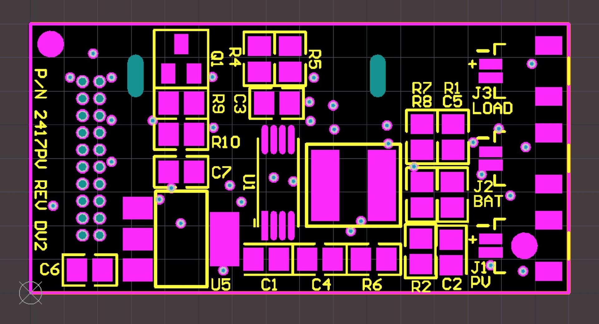
I generally use SMT components wherever possible, but for NanoSlot prototypes, I use thruhole connectors so that the hosts and modules align perfectly. (An added benefit is that my protos endure many insert/remove cycles, and this can be a strain on some SMT connectors, but is no trouble at all with thruhole connectors.) In production, of course, thruhole designs can be easily switched to SMT connectors.
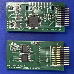
I might experiment with 3D-printing a carbon fiber jig to align SMT connectors perfectly for hand assembly. That would eliminate the need for respins.
Signals
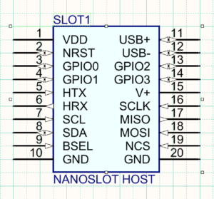
Electrically, NanoSlot provides multiple power options, USB, serial, I2C, SPI, and GPIO capabilities. It’s processor- and architecture-agnostic. I happen to use ST Microelectronics MCUs in my designs, but hosts can use other ARM processors, or RISC-5 processors, or even FPGAs with no processor core at all. In fact, I have several projects that use modules “freestanding” and others that use multiple modules bussed together with no host CPU at all.
The bus includes both common and point-to-point signals. The “common” side of the bus contains signals that are typically connected to all slots in a host: power, reset, I2C, and the clock and data lines for SPI.
Regarding “typically” : a host MCU with plenty of SPI ports can wire a dedicated SPI connection to each slot if desired, instead of using the same SPI bus for all slots. For that matter, it’s not at all a requirement that every module accepts SPI, nor is it a requirement that every slot provides SPI.
Likewise, one reset signal can be wired to all slots and also an MCU’s reset pin (so that every device in the design resets at once); alternately, the MCU can assign GPIO pins to each slot’s reset signal individually. Reset can also be bidirectional – a module can choose to reset its host, or vice versa. Some modules don’t use reset at all.
VDD is a dedicated power rail typically providing regulated 3.3V DC, but can be 1.8V or any other voltage that the host and all modules agree upon. VBUS is an undedicated and often unregulated power rail whose purpose can vary from one application to another. Possible uses include:
- A 3.7V wall wart
- A 5V USB input
- A 9V wall wart
- A 12V nominal vehicle supply
- A battery pack, such as a LiPo 4.2V cell
Check the specs on each module in your project to ensure there are no conflicts; so far, this hasn’t been a problem for me. Just in case, if a module uses or offers the VBUS rail, I include a zerohm jumper so that VBUS can be connected or disconnected on a per-module basis.
In addition to the common or shared signals, there are also point-to-point signals that must be unique to each slot: USB, serial, SPI select, and GPIOs. Again, any of these can be omitted: as an example, in a typical design, only one or two slots will provide USB. The GPIOs are also very loosely defined. I typically reserve GPIO0 for counter/timer/PWM uses, and I generally reserve GPIO1 for analog signals, but this is absolutely flexible.
One of these point-to-point signals is pin 9: BSEL, the “board select” line. This can be used several ways, but is intended mainly for use with the I2C bus. The I2C interface on each board includes an isolator; even though I2C chips have addresses so that they can share a bus, there is no guarantee that their addresses are unique. (Many parts can be strapped to different address ranges, but then again, many cannot.) By adding BSEL to specify which slot is targeted, all slots can use a single I2C host port, and still be guaranteed that there will be no address conflicts. A single board can (and often does) contain multiple I2C devices.
Firmware and Settings
Why is this important? Another feature of NanoSlot is that each module contains an I2C EEPROM for board identification and built-in software capabilities. Many EEPROMs use the same I2C address, and that’s convenient for discovery purposes, provided you can still read each one individually. To keep all the EEPROMs from trying to chatter at the same time, the host can assert BSEL to indicate which module it wants to talk to.
This part of the spec is somewhat fluid at present, but the EEPROM includes vendor ID and device ID (akin to USB), versioning information, application-specific configuration storage, and digital signature regions for authentication. It can also be used to store “device drivers” – I’ll post more about this in a future article.