Multi-megawatt renewable energy projects are all the rage these days, and with good reason. Having said that, is there such a thing as a renewable tech project that is too small?
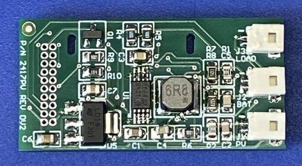
This little board is based on the SPV1040 boost charger by ST Microelectronics. Its mission is to efficiently harvest single digits of watts (or even fractions of a watt). Full throttle, it can accept 1.8 amps of input at up to 5.5 volts. On the low end, it’s happy to drink up milliamps at just half a volt. This makes it ideal for tiny sources like single solar cells, piezo crystals, micro wind and water turbines, and so on.
You’ll want to store those precious watts, and the SPV1040 provides current and voltage limiting that is suitable for lithium, NiCd, and NiMh batteries as well as supercapacitors.
My board pairs the SPV1040 with an ultra-low-power microcontroller: the STM32L072, another part from ST Microelectronics. The MCU monitors the voltage at the energy source and at the storage battery, and it can switch energy to two destinations independently: a two-pin connector for general purpose use, and a 20-pin NanoSlot connector for digital applications. The MCU can disconnect the loads and prevent overdischarge of the battery. For applications like landscape lighting, the MCU can provide “on-at-night” operation.
The L072 also sets up a great case study in very-low-power hardware and software design. Even clocking normally, it runs in the sub-milliamp range, However, by making full use of its analog peripherals and low-power standby/stop modes, I reduced its current below my ability to accurately measure.
About the design
Since this is a boost converter, it will typically be used with a single photovoltaic cell. It’s not meant for use with panels that already provide higher voltages than the battery pack; I have a separate design on my bench right now for use with larger panels.
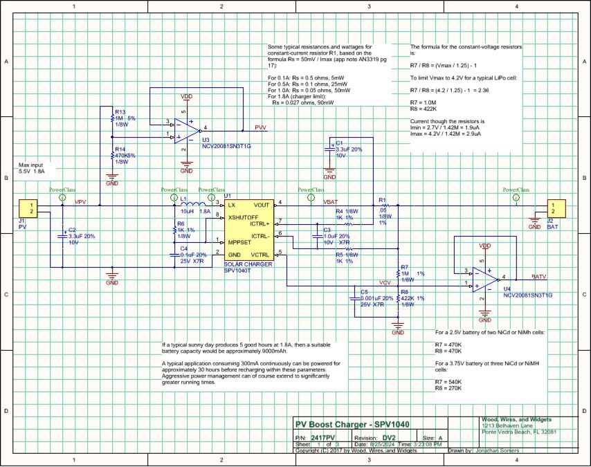
Sheet 1 features the heart of the design. The SPV1040 and inductor L1 provide the bulk of the boost converter. R6 and C4 govern the maximum power point (MPPT) operation of the 1040. ST’s datasheet and app note provide the shortest accurate description of MPPT that I’ve come across; ST describes it as an exercise in dynamic impedance matching.
C1 filters the boost output, and sense resistor R1 sets the current limit for the constant-current phase of charging. Sheet 1 has some notes on different values of R1 for various sizes of battery packs. C3, R4, and R5 couple the current sense resistor to the 1040’s sense inputs.
R7 and R8 set the voltage limit for the constant-voltage phase of charging. Again, the schematic provides some alternate values for two or three NiCd/NiMh packs. NiCds should do fairly well with this charger, but NiMh packs won’t provide optimal storage. Most NiMh chargers will slightly exceed the pack’s target voltage just before switching to trickle charge, and the SPV1040 doesn’t have provision for that algorithm.
Op-amps U3 and U4 simply buffer the voltage readings for the MCU’s A/D converter. They’re optional; if you’re building this design for yourself and you just want a boost charger with no MCU, you can omit them.
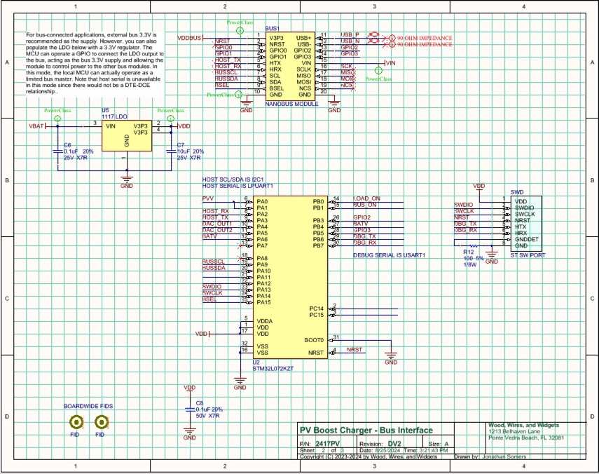
Sheet 2 includes the STM32L072 MCU (U2), its SWD programming port, a 1.8V LDO (U5) for the MCU, and a NanoSlot connector. All of these are completely optional if you just want to use the design for charging. Adding the MCU lets you manage a connected load, for features like automatic on-at-night operation, timed operation, and operation above a certain battery voltage.
If you’re using the charger in a NanoSlot design, you can power the MCU from the bus Vdd, in which case you can omit LDO U5 and tie the module’s Vdd to bus Vdd permanently. You can also go the opposite direction and power the bus from the LDO. If your bus-based design wants 3.3V as its main rail, you can substitute a pin-compatible 3.3V LDO, but remember that LDO stands for low drop-out, not zero drop-out. You’ll only be able to use a LiPo pack from its nominal 4.2V peak voltage down to about 3.7V, which is typically a fraction of its total capacity.
The MCU monitors both the PV voltage and the battery voltage. During hardware testing, I ran the MCU core at 1.024 MHz and monitored the voltages once per second via the A/D converter; the test code never put the MCU to sleep. Later, I optimized the code to turn off the high-speed clocks most of the time. Once per minute, the RTC wakes the MCU, which reads the ADCs, reports their values, and decides if any action is needed; then it’s back to “clocks off” to conserve power for the next minute. This puts the MCU drain in the sub-milliamp range.
However, it’s possible to do even better. The design also routes these sense voltages to the STM32L0’s built-in analog comparators. Once they have been programmed with threshold voltages, the MCU can stop executing code completely, turn off all peripheral clocks, and go into deep powersave mode (just preserving the GPIO outputs so that FETs Q1 and Q2 remain switched correctly). The comparators will interrupt and wake the MCU whenever action is needed.
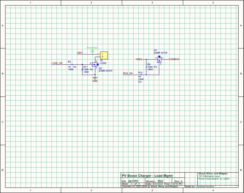
Sheet 3 provides the load management. The onboard MCU can turn on or off NFET Q2 to connect or disconnect the load to the unregulated battery voltage as needed. Similarly, the MCU can turn on or off PFET Q1 to connect regulated VDD (1.8V, or whatever you chose for your LDO) to the bus. The MCU should be programmed to provide undervoltage lockout and protect the battery pack from overdischarging.
Fabrication
I created this design with three different configurations in mind.
- If all I need is an efficient MPPT boost charger, I can populate just the top side of the module PCB. The SPV1040 will operate fine in this setup.
- If I want additional battery management system (BMS) features like undervoltage protection or load management, I can populate both sides of the board and write any custom MCU firmware that the application needs, right on the module.
- If I want to use this charger as a component in a larger system, I can add the NanoSlot connector, and even power the target system.
The two diagrams below show the board artwork. All the principle components for charging are on the top side of the board. Everything on the bottom side is optional.
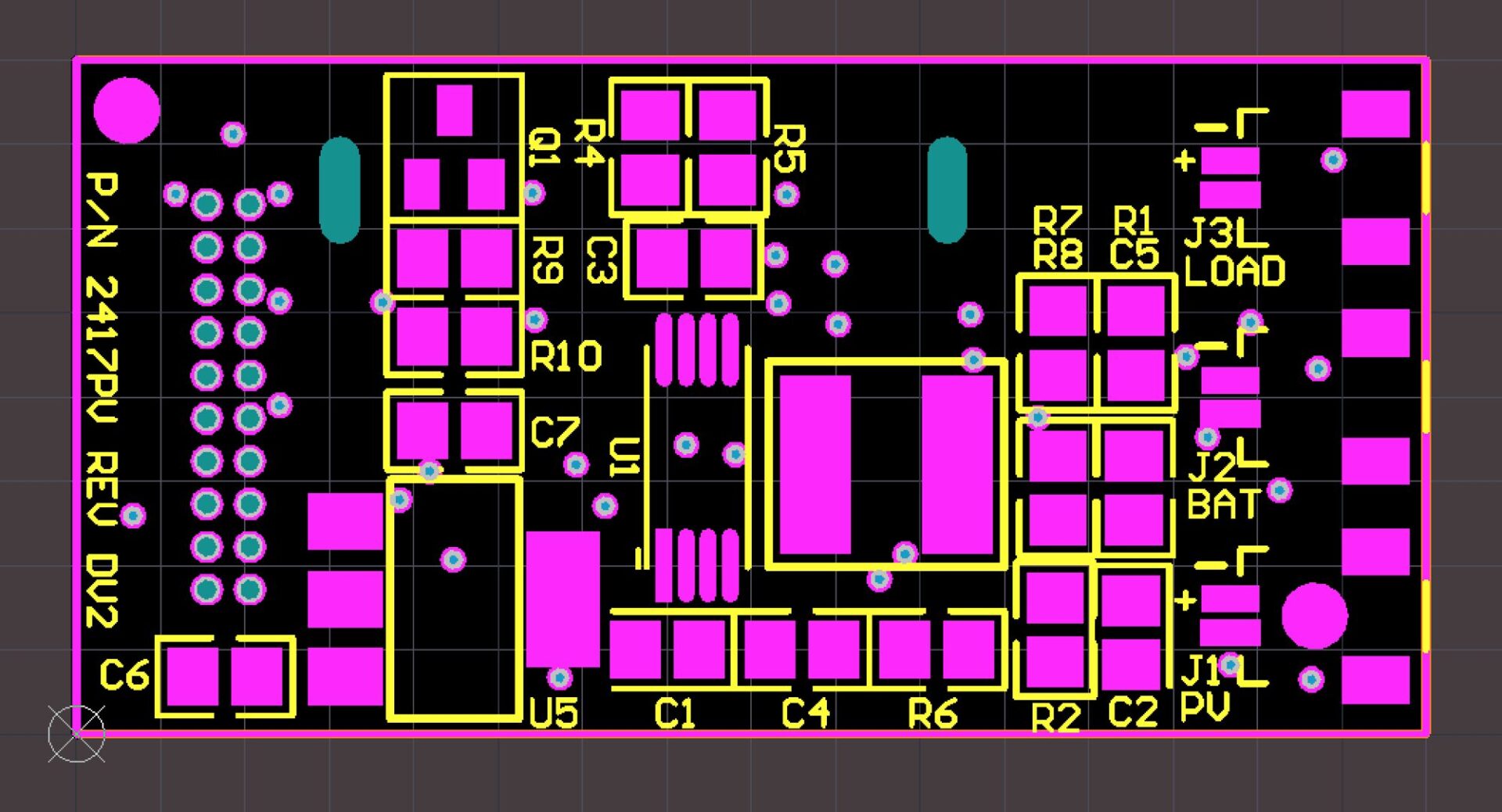
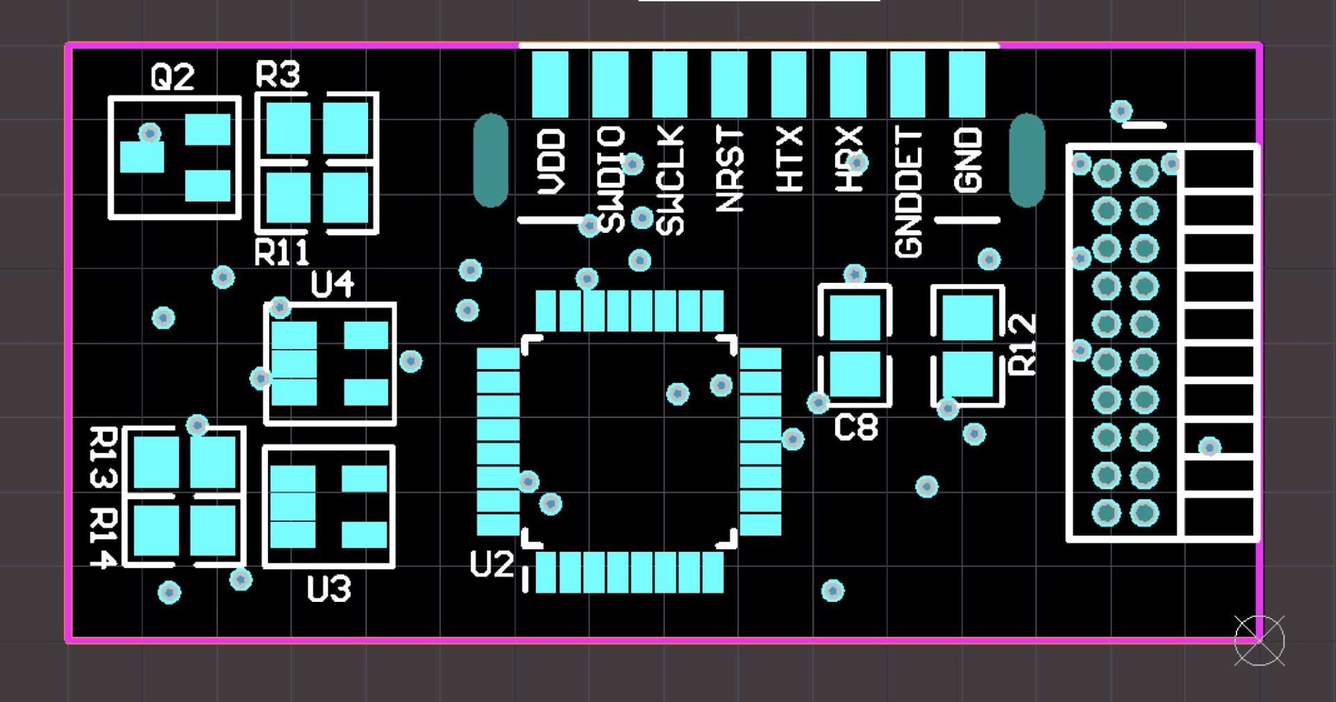
This board has been working really well, but I think I will do one more board spin in the near future. I’d like to add test points for rapid automated verification.
Pilot project
I used the second configuration above as the core of my upcycled solar yard light project, and I have been super pleased with the results so far. I am planning to use that same configuration with larger components to build a pair of solar-powered deck lights for our sailboat, Zen Chaser, I’d also love to use the design in other more complex projects, so stay tuned!